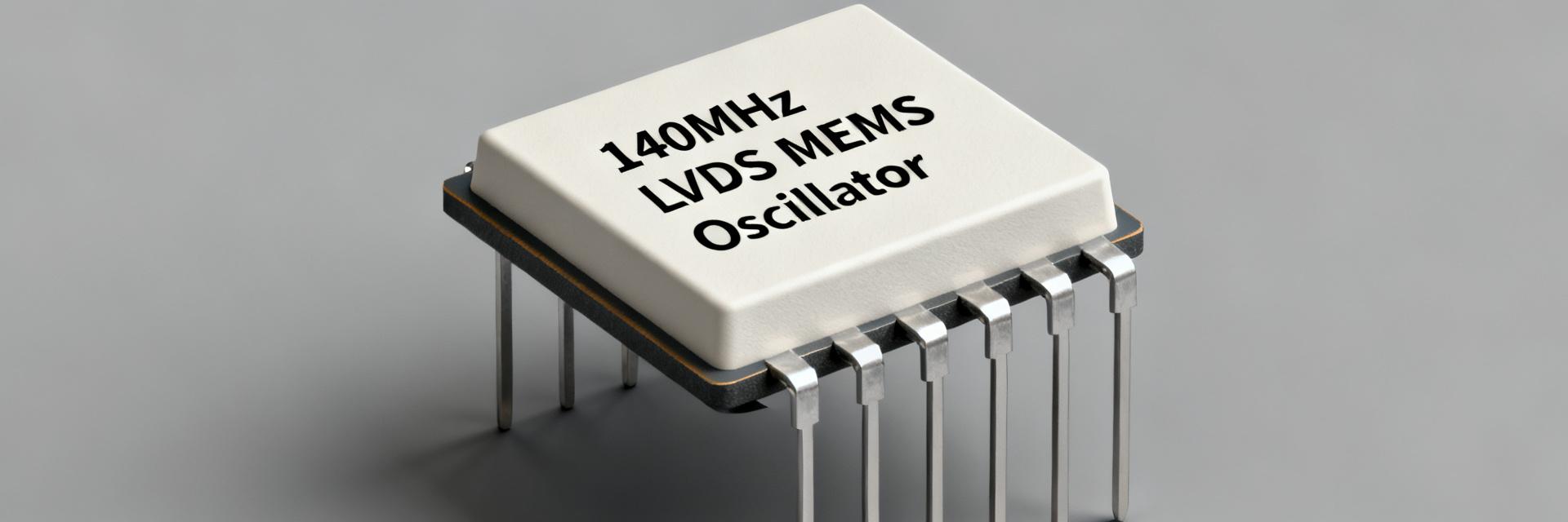
The DSA6111ML2B-026.0000TVAO is a 26.0000 MHz MEMS oscillator in a compact 2.0 x 1.6 mm 4-lead VFLGA-style package, designed for low-power clocking in space-constrained systems. Key headline numbers: 26.0000 MHz frequency, typical frequency stability ±25 ppm, operating voltage ~1.8–3.3 V, operating temperature range −40°C to +105°C, and a small active current in the low microamp to low milliamp range. This article consolidates the part’s datasheet figures and provides test and design guidance for verification and procurement.
Product overview & key specs (Background introduction)

The part is a MEMS-based oscillator/XO intended as a drop-in clock source for microcontrollers, communication PHYs, and consumer or industrial timing functions where small footprint and tight frequency control are required. Typical application constraints include limited board area, low supply voltage options, low standby power, tight thermal range operation, and immunity to supply noise.
What this part is and common applications
Point: This device is a MEMS oscillator offering an LVCMOS-like clock output in a very small package. Evidence: Its 4-lead VFLGA-style package and 2.0 x 1.6 mm footprint suit dense PCBs. Explanation: Use cases include MCU system clocks, USB/serdes reference clocks (when frequency matches system needs), real-time clocks in battery-powered devices, and industrial controllers requiring extended temperature operation.
At-a-glance spec card (quick reference)
Point: Quick reference specs aid rapid selection. Evidence: Frequency: 26.0000 MHz; stability: typ. ±25 ppm; supply: nominal 1.8 / 2.5 / 3.3 V or min/max per datasheet; package: 2.0 x 1.6 mm (0.079" x 0.063"), 4 leads; temp range: −40°C to +105°C; output: LVCMOS; lead count: 4. Explanation: Keep this table near your BOM and verification plan for fast cross-checks with board constraints and power budgets.
| Parameter | Specification Details |
|---|---|
| Nominal Frequency | 26.0000 MHz |
| Frequency Stability | ±25 ppm (Typical) |
| Supply Voltage (VDD) | 1.8V to 3.3V (Nominal) |
| Operating Temperature Range | −40°C to +105°C |
| Output Type | LVCMOS |
| Package Footprint | 2.0 x 1.6 mm VFLGA (4-lead) |
Electrical specifications: full datasheet specs (Data analysis)
Absolute and operating ratings set the safe envelope for design and soldering processes. Typical absolute maxima include max supply voltage, storage temperature limits, and maximum reflow temperature; recommended operating conditions list supply min/max and the guaranteed temperature range. Distinguish typical values from guaranteed limits when defining acceptance criteria.
Absolute ratings & operating conditions
Point: Identify limits that, if exceeded, can cause irreversible damage. Evidence: Common entries include VCC absolute max, storage temp extremes, and peak reflow temperature. Explanation: Use recommended operating voltages for reliability and apply derating for high-temperature applications; note soldering profiles and avoid exposing parts to package temps above recommended peaks.
AC & DC electrical characteristics to document
Point: The datasheet lists both DC and AC characteristics that must be captured in procurement specs. Evidence: Items include frequency accuracy/tolerance, ageing (ppm/year), frequency stability vs. temperature, supply currents (active/standby), output levels and timing (rise/fall), startup time, enable/disable behavior, jitter and phase noise. Explanation: Present typical and guaranteed columns in your internal spec sheet and define confidence intervals and test conditions for each measured parameter.
Measured performance & test data (Data analysis — lab results)
Reproducing key lab measurements ensures components meet system-level timing needs. Specify the exact test procedures, instrumentation, and sample sizes so results are comparable and defensible during supplier evaluation and incoming inspection.
Key lab measurements to reproduce (frequency, stability, jitter)
Point: Define repeatable tests for frequency, temp stability, and jitter. Evidence: Use a frequency counter with <1 Hz resolution or a phase noise analyzer for jitter; test at multiple temps (−40, 25, 85, 105°C), with n≥10 samples. Explanation: Record mean, standard deviation, and worst-case deviation; plot frequency vs. temperature and produce jitter histograms; label which values are typical versus guaranteed per the datasheet.
Environmental & mechanical test results
Point: Stress tests reveal latent weaknesses under field conditions. Evidence: Perform thermal cycling, humidity soak, and vibration/shock per your qualification plan; capture frequency shift and failure modes post-stress. Explanation: Report pre/post stress frequency, identify drift in ppm, log mechanical failures, and tabulate results to support lot acceptance criteria and design guardbands.
Application & PCB design considerations (Method/guide)
Power integrity and PCB layout materially affect oscillator performance. Proper decoupling and careful clock routing minimize noise coupling that increases jitter or causes frequency wander under dynamic loads.
Power, decoupling, and startup behavior
Point: Supply filtering reduces jitter and ensures reliable startup. Evidence: Recommend a high-quality 0.1 µF ceramic decoupling cap as close as possible to the VCC pin, optionally with a 1 µF bulk cap on the rail and minimal series inductance. Explanation: Place bypass caps within 1 mm of the part, avoid shared noisy power islands, and verify startup sequencing so the oscillator reaches stable output within the datasheet startup time.
Footprint, routing and grounding tips
Point: Footprint and return path quality influence solder reliability and signal integrity. Evidence: Use a defined land pattern with solder fillet allowance, a single solid ground plane under the part, and keep high-speed traces away from the package body. Explanation: Apply thermal reliefs if necessary, keepout areas for noisy components, and route clock traces with controlled impedance and length matching as required by downstream devices.
Reliability, qualification & screening (Method/guide / case)
Interpreting ageing and accelerated tests guides expected field behavior and sets procurement guardbands. Establish screening and lot acceptance tests to detect out-of-spec parts before assembly.
Interpreting reliability data and ageing
Point: Ageing is often quoted in ppm/year and requires context. Evidence: Convert accelerated test results to expected field drift using established models, and identify any systematic shifts vs. lot or date code. Explanation: If measured drift approaches your tolerance, establish a guardband in initial specification or plan for periodic recalibration where feasible.
Screening, lot traceability & sample acceptance criteria
Point: Incoming inspection prevents field failures from out-of-spec lots. Evidence: Recommend room-temp frequency checks, visual/polarity inspection, and solderability tests on samples; define sample size and acceptance numbers based on lot size and criticality. Explanation: Require supplier traceability (revision identifiers) and insist on matching ordering codes and package drawings to prevent cross-shipments.
How to obtain the latest datasheet & verify samples (Action recommendations)
Confirming the correct datasheet revision and performing a concise bench validation reduces risk before volume buys. A checklist and stepwise bench flow make verification repeatable across engineering and quality teams.
Datasheet validation checklist & version control
Point: Validate that the datasheet revision matches the ordered P/N. Evidence: Check PDF revision/date, revision notes, package drawing and pinout, and cross-check electrical tables. Explanation: Include a short template request to suppliers for revision history and confirm the ordering code and package prior to approval for production builds.
Practical bench test checklist for verification before production
Point: A compact bench flow accelerates qualification. Evidence: Steps: visual inspection → solder to test PCB → power-up and measure supply current → measure frequency at multiple temps → jitter/phase noise measurement → environmental stress checks. Explanation: Required instruments include a high-resolution counter, phase-noise analyzer or high-bandwidth scope, temperature chamber, and a vibration table if needed; define pass/fail thresholds in your incoming inspection plan.
Summary
- Consolidated key specs for the DSA6111ML2B-026.0000TVAO: 26.0000 MHz, typ. ±25 ppm stability, 1.8–3.3 V options, 2.0×1.6 mm package—use these as primary selection filters during procurement and board design.
- Test essentials: reproduce frequency vs. temperature, jitter histograms, and ageing checks with n≥10 samples; separate typical vs. guaranteed datasheet values and log worst-case deviations.
- Layout and power: place a 0.1 µF decoupler within 1 mm of VCC, maintain a solid ground plane, and keep high-speed traces out of the package keepout to minimize jitter and soldering issues.
- Qualification: require datasheet revision checks, incoming lot traceability, and a short bench verification flow before approving parts for production.
Frequently Asked Questions
What test equipment is required to verify oscillator specs?
Measure frequency with a high-resolution counter (sub-Hz resolution), use a phase-noise analyzer or high-bandwidth scope for jitter, and a temperature chamber for stability over temperature. Include n≥10 parts to capture lot variation and document mean, sigma, and worst-case for acceptance.
How should I set pass/fail limits for incoming lots?
Set pass/fail limits based on guaranteed datasheet bounds with a conservative guardband (e.g., 20–50% tighter for critical clocks). Use sample plans keyed to lot size and criticality and escalate failing lots to supplier review with documented readings and lot codes.
What footprint and soldering checks prevent assembly issues?
Follow the recommended land pattern with proper solder fillet allowance, use a controlled reflow profile below the part’s peak rating, and inspect solder joints on sample parts. Verify pad cleanliness and solderability during initial incoming inspection to avoid tombstoning or poor wetting.
What decoupling capacitor configuration is recommended for power integrity?
We recommend a high-quality 0.1 µF ceramic decoupling capacitor placed as close as possible (within 1 mm) to the VCC pin, optionally paired with a 1 µF bulk capacitor on the supply rail to minimize power supply noise and clock jitter.