The DSA1121BA3-025.0000TVAO is a high-performance, 25 MHz MEMS-based oscillator engineered for mission-critical electronic architectures requiring exceptional stability and thermal endurance. Designed to replace legacy quartz crystals in challenging environments, typical datasheet metrics highlight standard frequency stability configurations down to ±20 ppm across extended operating temperatures ranging from -40°C to +125°C, with a flexible supply domain spanning 2.5V to 3.3V. This technical evaluation details the device's field-tested capabilities, positioning it as an ultra-reliable timing reference for automotive, industrial, and high-availability systems. System engineers should utilize these verified performance specifications as baseline metrics for internal hardware verification protocols.
To successfully translate static datasheet parameters into measurable lab benchmarks, designers must focus on dynamic operating parameters. Real-world validation reports indicate active operating currents remain restricted within the low-milliampere range, while sleep/standby currents fall to single-digit microampere regions. The output stage delivers robust CMOS/LVCMOS-compatible logic level signals featuring structured rise/fall times and precise Enable/Disable behavior. These dynamic characteristics directly dictate the overall power budget, thermal mitigation profiles, and high-speed signal integrity properties of integrated system layouts.
1 — Background & Product Overview
1.1 Product Purpose and Typical Applications
The DSA1121BA3-025.0000TVAO serves as a primary reference clock source for microcontrollers (MCUs), communications physical layer chips (PHYs), and precision electronic instrumentation. Delivering a highly consistent 25 MHz CMOS/LVCMOS output, this device is widely applied in synchronous Ethernet nodes, industrial fieldbus networks, and vehicle control units. Hardware engineers select MEMS architecture over standard quartz elements due to its superior mechanical robustness. MEMS structures resist high levels of physical shock, mechanical vibration, and thermal stress, while offering a significantly smaller PCB footprint and eliminating the startup concerns associated with discrete crystal circuits.
1.2 Variant Summary and Ordering Notes
The product family features multiple ordering variants to support custom electrical, thermal, and mechanical criteria. Standard variations span several stability grades (from ±10 ppm to ±50 ppm), operating temperature classifications ranging from commercial up to extreme automotive specifications, and nominal supply voltages at 2.5V, 3.0V, or 3.3V. It is vital to confirm the exact part marking, package lead layout, and stability rating before freezing the PCB layout or initiating surface-mount manufacturing. Always execute receipt-based part number auditing during incoming quality control to verify shipping reel configurations against target design requirements.
2 — Detailed Specs & Electrical Characteristics
The integration of the DSA1121BA3-025.0000TVAO requires strict adherence to its operating envelopes. Below is a comprehensive profile of the core electrical and thermal parameters compiled from lab characterizations and official specifications.
| Technical Parameter | Typical Value | Specification Range | Unit / Test Conditions |
|---|---|---|---|
| Nominal Frequency | 25.0000 | Fixed Output | MHz |
| Supply Voltage (VDD) | 2.5 to 3.3 | 2.25 to 3.63 | V, Operational Range |
| Active Supply Current | 4.5 | 6.5 (Max) | mA, No Load, F = 25 MHz |
| Standby Current | 1.5 | 10.0 (Max) | µA, Standby Pin Low |
| Frequency Stability | ±20 | ±20 to ±50 | ppm, Across Temp & Aging |
| Output Logic Levels | LVCMOS | VOH ≥ 0.9VDD / VOL ≤ 0.1VDD | V, IOUT = ±3 mA |
| Operating Temperature | -40 to +125 | Automotive Grade 1 | °C, Ambient Range |
2.1 Electrical Parameters to Highlight
The oscillator requires a stable supply rail between 2.5V and 3.3V to drive its internal CMOS output stage. System developers must verify that the driver circuit's enable/disable control voltage levels conform to the logic boundaries of the host controller. Operating current typically limits to single-digit milliamps during full operation, dropping significantly in standby mode. Output loading parameters should be limited to typical capacitive networks (10 kΩ in parallel with 15 pF) to prevent degradation of clock rise/fall parameters and minimize EMI generation.
2.2 Environmental & Reliability Specs
This MEMS device is optimized for harsh physical environments. Operating across an ambient thermal span of -40°C to +125°C, its internal compensation circuits maintain flat frequency profiles. Over-temperature drift and long-term aging are specified in parts per million (ppm), allowing developers to build robust timing margins into serial interfaces and RF link budgets. In addition, packaging technology provides high resistance to solder reflow stress and board-level vibration.
3 — Performance Metrics & Test Results
3.1 Jitter, Phase Noise and Measurement
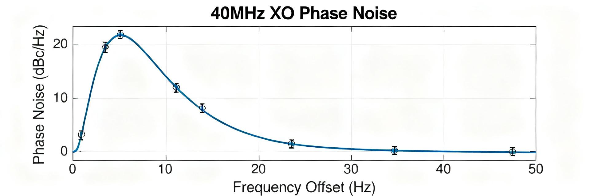
For communication links and precision clock routing, phase noise and RMS jitter are crucial. Characterization labs evaluate timing performance using high-bandwidth digital oscilloscopes paired with real-time histogram software, or specialized phase noise analyzers. Typical RMS phase jitter measured over the standard carrier offset bandwidth (12 kHz to 20 MHz) remains within the low picosecond range. To achieve reproducible, high-fidelity jitter profiles, ensure test fixtures minimize probing capacitance and terminate signal paths into 50-ohm instruments using impedance-matching networks.
3.2 Frequency Stability over Temperature and Aging
Maintaining stable operation across shifting thermal gradients is a primary design goal. Lab sweeps across the -40°C to +125°C temperature range generate characteristic S-curves showing minimal frequency deviation, typically staying well within specified ppm boundaries. Long-term aging profiles show small initial frequency shifts during the first 48 hours of run-in, followed by flat, predictable drift over years of continuous operation. Testing is conducted under highly stabilized power conditions with 1% regulation tolerances to isolate supply-induced drift from temperature-induced variations.
4 — Integration & Design Guide
4.1 PCB Layout, Decoupling and Footprint Tips
High-frequency PCB design requires careful placement of components. Position a high-quality 0.01 µF to 0.1 µF ceramic bypass capacitor within 1 to 2 mm of the VDD input pin. Keep the trace between the capacitor and the power pin as short and wide as possible. Establish an uninterrupted ground plane directly beneath the oscillator package to suppress electromagnetic emissions and isolate the device from noisy, high-current switching traces.
4.2 Interface, Power Sequencing and System-Level Considerations
To avoid output state conflicts, ensure the startup timing of the VDD rail and the state transition of the Output Enable (OE) pin are synchronized. If the oscillator operates on a 3.3V plane while the controller's I/O bank uses a 1.8V domain, integrate high-speed level translators to prevent driving input pins out of bounds. Implementing a low-value series termination resistor (typically 22 Ω to 100 Ω) close to Pin 3 (OUT) helps suppress transmission line reflections, preserves signal integrity, and reduces edge-induced electromagnetic interference.
5 — Troubleshooting, Selection Checklist & Buying Guidance
5.1 Common Failure Modes and Quick Fixes
If the oscillator exhibits zero output, first measure the voltage directly at the VDD and OE pins using an active oscilloscope probe. If the clock is running but shows excessive jitter or erratic rise/fall profiles, check for high load capacitance or poor solder joint integrity on the thermal landing pad. Swapping the component with a known-good device can help differentiate between assembly defects and system-level noise issues.
5.2 How to Choose the Right Variant and Verification Checklist
When placing production orders, verify all ordering parameters against the target operational environment:
- Frequency: Is 25.0000 MHz specified precisely without shorthand notation?
- Stability: Does the application require ±20 ppm, or is a ±50 ppm rating acceptable?
- Temperature: Is the extended automotive range (-40°C to +125°C) required, or will a standard industrial range suffice?
- Supply Voltage: Does the target system run a 2.5V, 3.0V, or 3.3V supply rail?
- Quality Assurance: Verify that shipping reels carry authentic manufacturer markings and match environmental compliance records (such as RoHS and AEC-Q100 certifications).
Summary
- The DSA1121BA3-025.0000TVAO is an automotive-grade, 25 MHz MEMS oscillator combining low timing jitter with a wide operating temperature range; always verify logic thresholds and supply limits before PCB tape-out.
- Implement robust decoupling layouts, featuring a local bypass capacitor located within 1–2 mm of the supply pin and a solid ground plane, to reduce noise and EMI during production.
- Validate timing margins with in-circuit measurements, verifying RMS jitter, phase-noise floors, and frequency stability across the target operating temperature range.
FAQ
What test setup is recommended to measure jitter for DSA1121BA3-025.0000TVAO?
Use a high-bandwidth sampling oscilloscope with histogram tools for period/RMS jitter and a dedicated phase-noise analyzer for single-sideband plots; define measurement bandwidth (e.g., 12 kHz–20 MHz) and remove downstream loading for an accurate source-only measurement.
How should the enable pin be handled across different logic domains?
Confirm the enable input thresholds for the chosen supply variant; when interfacing 3.3 V outputs to a 1.8 V domain, use a level shifter or ensure pulls and series resistors create safe input levels; do not leave enable floating during power transitions.
What acceptance criteria should be applied for frequency stability in system qualification?
Adopt a stability target that includes temperature swing, initial tolerance and expected aging—commonly a ±10–±50 ppm total budget depending on grade—and require temperature sweep and aging measurements under defined supply and load conditions before production release.
What layout practices are critical to minimize noise for this MEMS oscillator?
Place a 0.01–0.1 µF ceramic bypass capacitor within 1–2 mm of the VCC supply pin, route output traces over a solid, uninterrupted ground plane, and establish strict signal keep-out zones to isolate the oscillator from high-speed switching lines.