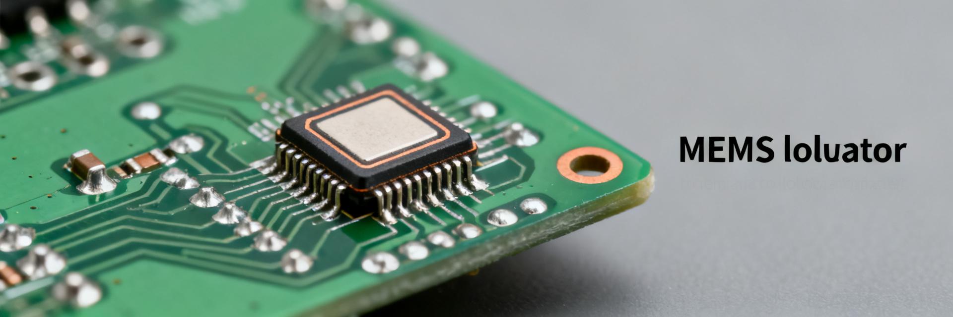
Point: The published datasheet for this 32.768 kHz oscillator family lists supply ranges near 1.71–3.63 V, standby/active currents roughly 1.3–3 mA, and frequency stabilities to ±150 ppm across −40 to +85 °C, metrics that directly govern battery life and RTC accuracy. Evidence: those numeric bands appear repeatedly in the electrical and timing tables. Explanation: translating these rows into system-level budgets is the first design task.
Point: This deep dive decodes those tables and graphs into concrete design actions. Evidence: practical items—revision checks, margining, measurement recipes, and a pre-production test list—derive from spec entries and plots. Explanation: follow the checklist here to turn datasheet numbers into reproducible validation and robust integration.
1 — What the Datasheet Actually Contains (how to read it)
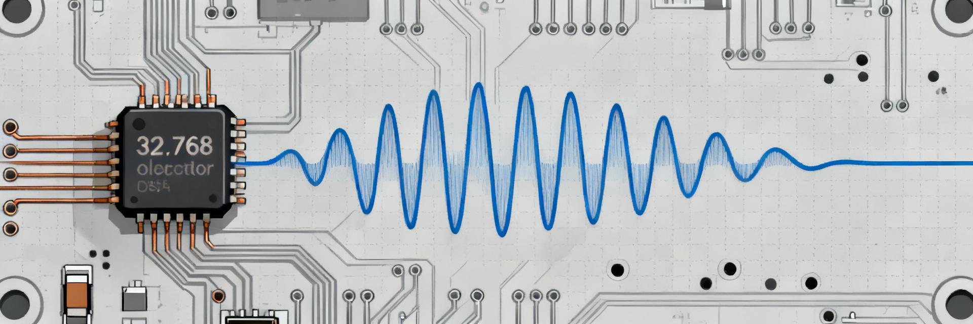
1.1 Document structure & revision notes
Point: Datasheets bundle identification, ordering codes, revision history and spec tables; the part-number suffixes encode package and option differences. Evidence: the header and revision table normally list document version and ordering codes. Explanation: action—confirm the latest revision and cross-reference the exact order code on your BOM to avoid subtle spec deltas or obsolete-marked items.
1.2 Absolute ratings vs. recommended operating conditions
Point: Absolute maximums are stress limits, while recommended operating conditions define the design envelope. Evidence: the absolute section lists max Vcc, junction temperature, and ESD thresholds; the recommended section gives nominal Vcc and temperature ranges. Explanation: action—design rails with ≈10% headroom under max ratings, and add ESD protection and thermal margin in the BOM.
2 — Key Electrical Specs: Power, Output & Frequency (interpretation + impact)
2.1 Supply voltage, output format and current consumption
Point: The datasheet specifies nominal and min/max supply (e.g., 1.71–3.63 V) and output as logic-level clock; peak and typical currents differ by mode. Evidence: typical active currents around 1.3–3 mA and lower standby currents are listed in the power table. Explanation: for DSA6101MA1B-032K768TVAO estimate battery life by converting current into mAh: a 3 mA active draw continuous equals ~26,280 mAh/year; duty-cycle and standby current dominate real-life battery life. Action: measure currents at specified Vcc, temperature and with defined load to reproduce datasheet numbers.
2.2 Frequency spec: 32.768 kHz accuracy, stability, load & drive strength
Point: Frequency specs cover initial tolerance (ppm), temperature stability curves, load capacitance and drive strength—each alters timekeeping error. Evidence: tables give initial ppm and graphs show frequency vs. temperature; output drive numbers indicate loaded edge slew. Explanation: action—verify 32.768 kHz at system temperature extremes, test with intended MCU input threshold and the actual load capacitance to ensure waveform integrity and timing accuracy claimed in the datasheet.
3 — Timing, Temperature Behavior & Reliability Data
3.1 Start-up time, jitter and timing tolerances
Point: Start-up time and jitter specs determine how quickly a reliable clock is available and how stable period-to-period timing is. Evidence: the timing section lists start-up to valid output and gives jitter and period stability numbers. Explanation: action—capture start-up on an oscilloscope (single-shot or triggered) at required Vcc and temperature; use a sampling scope with at least 1 MS/s effective sample for 32.768 kHz to quantify cycle jitter against datasheet limits.
3.2 Temperature curves, aging and environmental limits
Point: Temperature vs. frequency plots and aging specs predict worst-case RTC drift over product life. Evidence: plots show quadratic or S-shaped deviation across −40 to +85 °C and aging is given in ppm/year. Explanation: action—derive worst-case error budget by summing initial tolerance, temp delta and aging; apply derating (e.g., ±20–30% extra ppm) if product operates beyond qualified temperature or in high-humidity environments, and follow recommended reflow profiles in the mechanical/assembly notes.
4 — PCB Integration & Electrical Design Best Practices
4.1 Power routing, decoupling and enable/disable handling
Point: Proper Vcc/GND routing and decoupling are essential to meet the datasheet current and jitter specs. Evidence: layout recommendations typically show short Vcc traces and a local decoupling capacitor. Explanation: action—place a 0.1 µF ceramic close to Vcc pin and add a 1 µF bulk cap nearby, keep traces short, and if an enable pin exists use a defined pull resistor to set state during power sequencing; add a series ferrite or resistor for very noisy rails.
4.2 Footprint, soldering and package handling
Point: Small VLGA-style packages demand accurate stencil and pad design to avoid tombstoning and solder voids. Evidence: mechanical drawings give pad dimensions and recommended stencil aperture percentages. Explanation: action—use the recommended pad footprint, 60–80% paste stenciling for small pads, and observe placement force limits, ESD precautions, and post-reflow cleaning guidance to minimize solder-related failures.
5 — Application Examples, Comparisons & Final Design Checklist
5.1 Typical applications and comparative trade-offs
Point: This oscillator suits battery-backed RTCs, low-power IoT nodes and wearables where small size and moderate accuracy matter. Evidence: power and stability numbers favor integrated oscillator over discrete crystal in some board-space-constrained designs. Explanation: action—choose this part when compact package and integrated logic-level output outweigh the higher long-term accuracy of a temperature-compensated crystal; provide an mAh·year example using your duty cycle to compare options.
5.2 Implementation checklist & troubleshooting flow
Point: A tight pre-production checklist prevents late surprises. Evidence: common failures map to wrong order code, bad footprint, missing decoupling, or enable pin mis-wiring. Explanation: action—must-test bench items: (1) confirm doc revision and order code; (2) measure idle/active current at Vcc; (3) verify 32.768 kHz at three temperatures; (4) capture start-up time; (5) measure jitter; (6) inspect solder joints X‑ray/optical; (7) validate EN logic; (8) run long-term aging soak. Troubleshooting: if frequency off check Vcc tolerance, load, and temperature first; if no output check EN and solder continuity.
| Option | Size | Accuracy |
|---|---|---|
| Crystal | Medium | ±20–50 ppm (stable) |
| MEMS Oscillator | Small | ±50–±150 ppm |
| Integrated RTC | Varies | Function-rich, power trade-offs |
Summary
- Confirm the DSA6101MA1B-032K768TVAO key specs—32.768 kHz nominal, ~1.71–3.63 V supply, and listed current/stability figures—and convert them into battery and RTC error budgets before component selection.
- Follow layout and decoupling recommendations: local 0.1 µF + 1 µF caps, short Vcc/GND traces, defined EN pin state, and correct stencil aperture for the VLGA footprint to match datasheet performance.
- Execute the pre-production test plan: verify revision/order code, measure currents at specified conditions, validate frequency vs. temperature, capture start-up and jitter, and run the eight must-test bench items prior to mass assembly.
How should I test the 32.768 kHz frequency against the datasheet?
Point: Reproduce datasheet conditions to validate frequency and stability. Evidence: the datasheet gives test Vcc, load, and temperature points. Explanation: use a counter or high-resolution frequency meter with the part powered at the specified Vcc and the intended load, record results at three or more temperatures across the operating range, and compare ppm deviation to the datasheet limits; log results in your QA system.
What measurement setup verifies start-up time and jitter?
Point: Proper oscilloscope settings reveal start-up and jitter behavior. Evidence: timing specs reference start-up-to-valid and cycle jitter metrics. Explanation: trigger on the Vcc edge or enable transition, capture the first several cycles with a sample rate that yields >100 samples per cycle, measure time to first stable edge for start-up, and compute cycle-to-cycle and period jitter statistics to compare with datasheet values.
If the oscillator output is absent, what are the first steps?
Point: Systematic checks quickly isolate common faults. Evidence: missing output often stems from enable state, soldering, or incorrect Vcc. Explanation: first verify the enable pin logic and Vcc level with a multimeter, inspect solder joints and continuity to ground, confirm footprint alignment, and probe with a high-impedance scope input; replace the part with a known-good sample if the board checks out to rule out component-level defects.
Why is proper power decoupling critical for the DSA6101MA1B-032K768TVAO?
Point: Proper Vcc/GND routing and decoupling are essential to meet the datasheet current and jitter specs. Evidence: layout recommendations show short Vcc traces and a local decoupling capacitor. Explanation: placing a 0.1 µF ceramic close to Vcc pin and a 1 µF bulk cap nearby keeps the power line clean from high-frequency noise, which directly prevents clock phase noise degradation and spurious startup failures.