Point: The DSA1203DA3-100M0000VAO is specified as a 100 MHz LVDS output oscillator with tight frequency tolerance and low phase noise, making it suitable for high-speed digital clocking. Evidence: Datasheet figures list nominal 100.000 MHz frequency, LVDS differential output, supply range around typical 3.3 V, temperature grades spanning industrial ranges, ppm-level initial tolerance and sub-picosecond typical phase jitter. Explanation: Those numbers directly affect clock integrity for SERDES timing, PLL references and system BER budgets, so designers must read specs before integration.
Product overview and key specs (background introduction)
1.1 At-a-glance spec table
| Parameter | Typical | Min / Max | Units |
|---|---|---|---|
| SKU | DSA1203DA3-100M0000VAO | ||
| Frequency | 100.000 | ±var ppm | MHz |
| Output | LVDS | — | diff Vp-p / Vcm |
| Supply Vcc | 3.3 | 2.97 / 3.63 | V |
| Operating Temp | — | -40 / +85 | °C |
| Initial tolerance | ±25 | ±50 | ppm |
| Typical phase jitter (RMS) | ~0.2–0.6 | — | ps (12 kHz–20 MHz) |
| Duty cycle | ~50% | ±5% | % |
| Standby / Power-down | Yes | — | control pin / µA |
Point: Each listed parameter has practical implications for system design. Evidence: The datasheet tables and curves define tolerance vs. temperature, jitter bandwidths and supply current. Explanation: Supply rails determine required decoupling and regulator margins; ppm tolerance and temp coefficients govern whether the oscillator meets timing budgets across operating conditions; jitter specs constrain allowable noise for SERDES and ADC/DAC sampling.
Electrical performance deep-dive (data analysis)
2.1 Frequency accuracy, stability and temperature behavior
Point: Nominal 100 MHz frequency is only the starting point; stability over temp and supply sets long-term usefulness. Evidence: Initial frequency tolerance (ppm) and frequency vs. temperature curves in the datasheet show typical drift across specified grades and recommended test conditions (Vcc = 3.3 V, specified load, ambient). Explanation: When using a 100MHz LVDS oscillator as a PLL reference, account for ppm stacking (initial tolerance + temp drift + aging) and define test conditions—measure at regulated Vcc, with matched load and at target ambient temperatures to reproduce datasheet numbers.
2.2 Jitter, phase noise and timing integrity
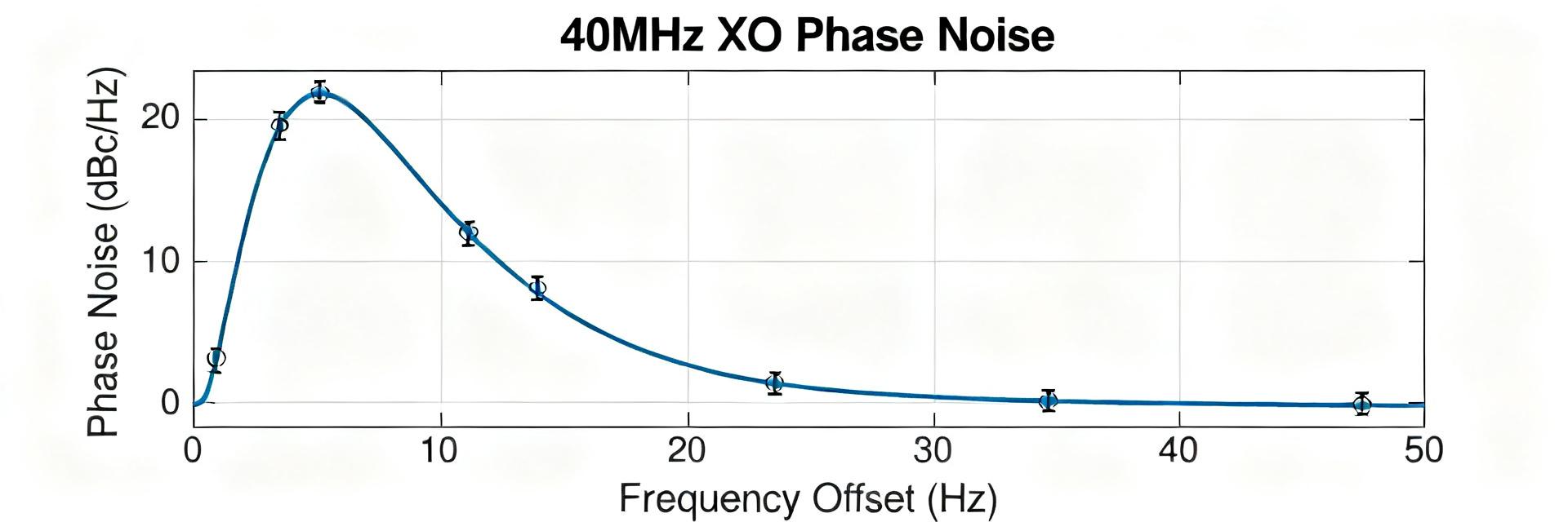
Point: RMS jitter and phase noise determine clock quality for high-speed links. Evidence: Typical RMS jitter values in the datasheet are given for a measurement bandwidth (commonly 12 kHz–20 MHz); phase noise curves indicate close-in noise that affects PLL lock. Explanation: Designers should compare the 100MHz LVDS oscillator jitter specification to system budgets: a 0.3 ps RMS oscillator contributes to the total TIE budget and can reduce SERDES eye margin. Measure with high-bandwidth scope plus jitter analysis software, using the same bandwidth as the datasheet to align expectations.
Electrical interface & power characteristics (method/guideline)
3.1 LVDS output behavior and load considerations
Point: LVDS outputs require controlled differential routing and correct termination to achieve the stated amplitude and common-mode behavior. Evidence: Typical differential amplitude and common-mode ranges are shown as operating values for the LVDS driver; recommended 100 Ω termination across the receiver inputs is the standard. Explanation: Mismatched load or omitted termination will reflect energy, distort edges and can increase measured jitter; ensure receiver input common-mode range is compatible and use matched pairs to preserve duty cycle and edge symmetry.
3.2 Power supply, standby modes and thermal notes
Point: Power characteristics and thermal limits determine reliability and margin for continuous operation. Evidence: Supply current and standby current figures in the datasheet give baseline consumption; recommended decoupling values and layout notes indicate supply decoupling close to pins. Explanation: For guidance on DSA1203DA3-100M0000VAO power consumption, budget BOTH active and standby currents, place bypass capacitors near Vcc, and plan thermal relief via copper pours and vias to keep junction temperature within limits under worst-case ambient.
Mechanical, packaging and board-integration guidance (case study / practical)
4.1 Package dimensions, footprint and mounting best practices
Point: Proper footprint and soldering profile prevent mechanical stress and ensure electrical reliability. Evidence: Package drawings specify pad locations, solder-mask recommendations and maximum height; reflow profile notes indicate maximum peak temperature and recommended ramp rates. Explanation: Use the recommended footprint with solder fillets, follow the specified reflow profile to avoid warpage, and consider component height when stacking or placing shields near the clock to prevent mechanical interference with high-speed routing.
4.2 Layout checklist for optimal clock integrity
Point: A short, practical checklist reduces integration risk when placing a high‑quality LVDS clock on PCB. Evidence: Best practices include differential pair length matching, controlled impedance, ground/power via stitching and decoupling near supply pins. Explanation: Follow this checklist for how to place 100MHz LVDS oscillator on PCB: route differential traces with 100 Ω differential impedance, keep pair separation tight, place 0.1 µF and 1 µF decouplers within 1–2 mm of Vcc pin, route return planes under traces, and keep noisy switching domains physically separated.
Use cases, selection tips and troubleshooting (action recommendations)
5.1 Typical applications and selection criteria
Point: Select this oscillator when low jitter and LVDS output are required for timing-sensitive systems. Evidence: Typical application areas include FPGA/ASIC references, telecom timing and high-speed logic clocking where ppm and jitter figures must meet link budgets. Explanation: When choosing a part, compare ppm, temp grade, package and standby options against system requirements, consult the datasheet frequency/temperature curves and validate by measuring in the target environment before finalizing the selection.
5.2 Common failure modes and debug steps
Point: Integration issues often stem from termination, supply sequencing or thermal stress. Evidence: Common reported problems include missing clock output, excessive jitter, duty cycle distortion or part overheating; diagnostic steps in practice use scope differential probes, termination checks and supply ramp monitoring. Explanation: For DSA1203DA3-100M0000VAO troubleshooting tips, capture differential scope traces, verify 100 Ω termination, monitor Vcc during power-up, inspect solder joints and confirm part temperature; adding small RC filtering or adjusting sequencing often resolves marginal cases.
Conclusion / Summary
- DSA1203DA3-100M0000VAO delivers a nominal 100 MHz LVDS clock with ppm-level accuracy and sub-picosecond-class typical jitter; confirm exact values in the datasheet before deployment.
- Design tips: use matched 100 Ω differential routing, tight decoupling at Vcc, and adhere to recommended reflow profiles to preserve signal and mechanical integrity.
- Validation steps: measure frequency, jitter (matching datasheet bandwidth), and power behavior under target temperature and load to ensure clocks meet system budgets.
- Troubleshoot by checking termination, supply sequencing and thermal conditions; use differential probing and jitter analysis for root-cause identification.