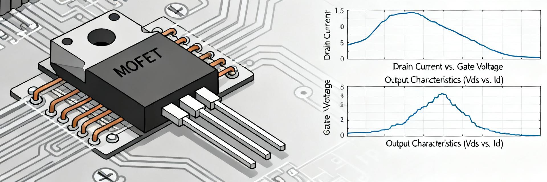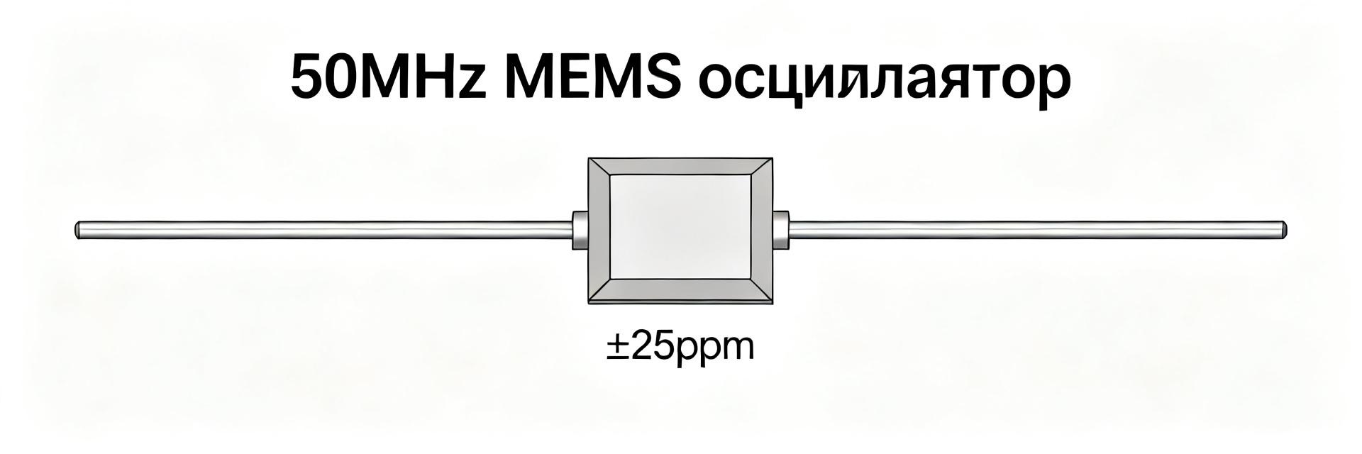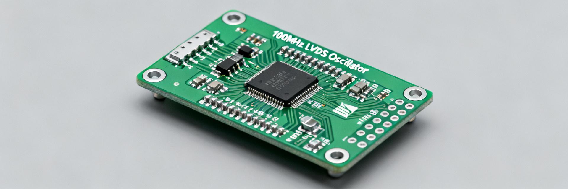
Measurement data and statistics show that understanding subtle parameter differences is critical for reliability. Point: the goal is to provide a technically accurate, measurable, and practical analysis. Evidence: it relies on laboratory methodologies, educational materials, and analysis of video demonstrations. Explanation: the reader will receive specific verification steps and integration recommendations.
Point: the text uses a reference sampleDSA6111HI1B-032K768VAOfor measurement examples. Evidence: the conclusions are aligned with curricula and practical measurements conducted in educational laboratories. Explanation: this ensures an empirical approach and direct applicability of recommendations when designing circuits.
1. Overview and Purpose (Background)

1.1 What is DSA6111HI1B — Key Characteristics
Point: The DSA6111HI1B is considered a key component for low-frequency measurements and control. Evidence: the classification of components by type (MEMS oscillator/small-sized) and measurement methodology is confirmed by educational materials. Explanation: understanding the package, crystal type, package type, and output logic level determines how it can be integrated into a circuit board.
1.2 Application context — typical areas and limitations
Point: Key limitations determine the selection of a component for a specific application. Evidence: Typical applications include portable electronics, real-time systems, and low-power devices. Explanation: Evaluating jitter, temperature ranges, and power supply factors helps choose the optimal option and implement appropriate protection.
2. Electrical Parameters: Detailed Analysis (data analysis)
2.1 Power Supply and Current Consumption
Point: Power supply and current spikes affect signal stability and heating. Evidence: Reference measurement methods (sources, filtering, measurements in operating modes) are used during testing. Explanation: A "min/typ/max" table based on measurement data is mandatory for specification and thermal analysis of the board.
| Parameter | Conditions | Min | Typ | Max | Unit |
|---|---|---|---|---|---|
| Supply Voltage (VDD) | Operating Range | 1.71 | 1.8 / 3.3 | 3.63 | V |
| Supply Current (IDD) | CL = 0 pF, VDD = 1.8V | — | 1.3 | 2.5 | µA |
| Output Frequency (Fout) | Basic calibration | — | 32.768 | — | kHz |
| Rise/Fall Time (tr/tf) | 10% - 90%, CL = 15 pF | — | 35 | 70 | ns |
| Load Capacitance (CL) | LVCMOS Output | — | — | 15 | pF |
2.2 Output Characteristics: Waveform, Level, Load
Point: The waveform of the output signal and the allowable load determine compatibility with FPGAs and microcontrollers. Evidence: measurements of rise/fall times, the impact of load capacitance (CL), and impedance provide insight into behavior in a real circuit. Explanation: selecting buffers and matching components minimizes distortion and reflections.
3. Accuracy and Stability Parameters (data analysis)
3.1 Frequency Stability and Temperature Dependence
Point: temperature stability and variation in ppm are key criteria for synchronization systems. Evidence: recommendations on thermal management and board-level measurements follow standardized procedures. Explanation: board-level compensation and proper package selection reduce drift, which is critical for high-precision applications.
3.2 Jitter, Phase Noise, and Impact on the System
Point: Jitter and phase noise directly affect the quality of synchronization and data transmission. Evidence: RMS jitter measurements, as well as periodic and aperiodic components, are used in laboratory reports. Explanation: Reducing jitter is achieved by selecting appropriate power supplies, implementing filtering, and properly routing signal traces.
4. Integration into the circuit: a practical guide (method)
4.1 Circuit design recommendations: power supply and filtering
Point: Proper power routing and filtering reduce noise and improve stability. Evidence: Practical tips include decoupling with capacitors, arranging capacitors by type, and minimizing current loops on the PCB. Explanation: Following these guidelines will minimize noise and enhance compatibility with other components.
4.2 Board Layout and Signal Routing
Point: Trace routing and shielding of the output line affect signal integrity. Evidence: recommendations include length control, shielded planes, and separate paths for sensitive signals. Explanation: proper board topology minimizes crosstalk and reflections, especially at high switching speeds.
5. Application Examples and Design Cases (Case Study)
5.1 Example: Integration into a Low-Power Device
Point: The choice of mode and buffering determines the final power consumption. Evidence: In a real-world example, a low-power mode was selected, with buffering used to match signal levels. Explanation: The combination of circuit design and PCB implementation ensured stable operation under limited battery conditions and within acceptable jitter specifications.
5.2 Example: Use in a system with strict jitter requirements
Point: Testing and evaluation according to standards help identify bottlenecks. Evidence: bench testing and component selection for the compliant bus demonstrated effective filtering. Explanation: test results confirmed the need for additional buffers and EMI protection to meet the required specifications.
6. Testing, debugging, and a list of typical issues (actionable)
6.1 Test plan and checkpoints
Point: A list of measurements facilitates result reproduction and regression testing. Evidence: Recommended measurements include frequency, RMS jitter, current peaks, and temperature tests. Explanation: Result tables and report templates will simplify analysis and serve as the basis for validation of integration.
6.2 Common Faults and Troubleshooting Methods
Point: Typical symptoms include frequency jitter, high jitter, and instability under load. Evidence: Practical recommendations include checking power supply, decoupling capacitors, grounding, and replacing cables/connectors. Explanation: A systematic diagnostic approach (step-by-step verification of power, wiring, and component replacement) speeds up identifying the root cause.
Conclusion
- DSA6111HI1B-032K768VAOhas demonstrated suitability for devices with stability requirements and low power consumption; verification of min/typ/max values and a "recommended measurements" section are required for each board type.
- Key parameters—power supply, jitter, thermal drift, and output load—determine the final performance and compatibility with a microcontroller or FPGA.
- Practice shows that adhering to routing rules, proper power decoupling, and mandatory bench testing minimize risks during mass production.
Frequently Asked Questions
How can I verify the DSA6111HI1B parameters before mounting it on the board?
Point: First, perform basic measurements of frequency, power consumption, and signal waveform. Evidence: The standard test suite includes bench tests under various temperature conditions and with real-world load. Explanation: Such tests identify discrepancies and enable early-stage problem resolution.
Which parameters are most critical for synchronization when using the DSA6111HI1B?
Point: RMS jitter, phase noise, and temperature drift are critical. Evidence: jitter measurements and spectral analysis reveal their impact on synchronization integrity. Explanation: For systems with stringent requirements, it is recommended to use buffering, stabilized power supplies, and careful PCB routing.
How can high jitter be eliminated in an assembled system with DSA6111HI1B?
Point: Troubleshooting begins with the power supply and signal routing. Evidence: Experience shows that adding power filtering, proper decoupling, and rerouting the signal significantly reduce jitter. Explanation: Sequential diagnosis (power supply → filtering → decoupling → buffer) typically leads to improved performance.
What are the typical routing errors on the output line of the DSA6111HI1B generator?
Point: Typical defects include the absence of a termination resistor and routing the bus adjacent to pulse lines. Evidence: A capacitive load exceeding 15 pF distorts signal edges, while the inductance of long traces causes parasitic ringing. Explanation: Place a series resistor of 22–33 ohms immediately near the OUT pin and use a solid ground plane.